Wafer Processing for High Topography Bumped Wafers: Conforming, Stress-Free Temporary Bonding Adhesive
Backgrinding and Wafer processing temporary bonding adhesives face additional challenges when used with bumped wafers.
- Difficult to absorb bumped contacts
- Bumps from 30 µm to 200 µm
- Solid-forming liquid based adhesives:
- 2 or more addition steps required for bumped wafer processing
- May include “back-milling” to level out an uneven adhesive layer
AI Technology, Inc. provides innovative solutions to meet this challenge.
- Peel-release temporary bonding adhesive: melt-conformal adhesive film on disposable carrier
- Adhesive layer thickness:
- For flat wafers:
- 20 µm adhesive layer
- For stud bumped and solder bumped wafers:
- 100 µm, 200 µm, or 400 µm adhesive layer – dependent on bump size
- For flat wafers:
- Adhesive layer Total Thickness Variation (TTV) < 2um
- Peels off cleanly with no residues
- No post process cleaning needed
- Melt-conforming-bonding process with disposable carrier:
- temperature: 140-150ºC
- pressure: <14 psi or rolling lamination
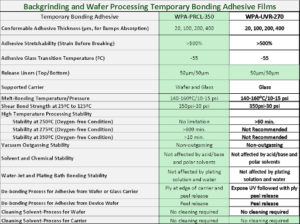
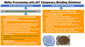
For use with traditional glass and wafer carrier: AI Technology, Inc.’s two novel temporary bonding adhesive solutions simplify the processing and increase wafer throughput:
- Clean Peel-Release Stress-Free Temporary Bonding Adhesive Film: WPA-PRCL-350
- UV Clean Release Temporary Bonding Adhesive Film: WPA-UVR-270
For use with a disposable carrier for multiplying the wafer throughput:
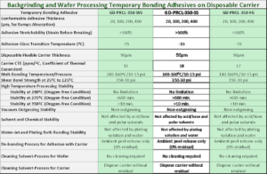
AIT patent-pending temporary bonding adhesives on disposable carrier:
- GD-PRCL-350-WS uses a disposable carrier that is closely matched to that of the device wafer such as silicon.
- GD-PRCL-350-SS uses a disposable carrier that is not as closely matched to that of the device wafer.
- GD-PRCL-350-FG uses a proprietary high temperature carrier
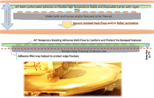
Melt-Conformable and Bump Encapsulating Wafer Processing Temporary Bonding Adhesive:
Temporary bonding adhesive must melt and conform to absorb and encapsulate all of the bumps and features of the device wafer without stress. These criteria are critical for the success of backgrinding; if the adhesive does not meet these requirements the bumps will be reflected on the backside.
AIT temporary bonding adhesive films WPA-PRCL-350 and GD-PRCL-350-WS:
- pre-deposited onto disposable carrier
- Molecularly engineered for high flexibility: eliminates need for CTE matched carrier
- High melt-flow indices at 140-160ºC
- Conform to the highest of bumps, up to 200µm.
AIT disposable carrier solutions offer powerful advantages:
- Much higher wafer throughput
- Eliminate cost, time, and resources for carrier bonding, debonding, and cleaning
- Optimized gain and simplification in 3D wafer processing
- Multiplies typical throughput of 20 wafers/hour
AIT’s patent pending melt-conformable temporary bonding adhesive on disposable carrier is molecular designed to have extreme flexibility. It allows conformity without inducing interfacial stress, even without CTE matched carrier wafer.
Film format availability for wafer processing temporary bonding adhesives eliminate dispensing, drying, and post leveling machining processes. Residue-free release from both the device wafer and carrier avoids cleaning processes and saves time, especially compared to focused laser ablation methods. The use of disposable carrier provides even greater efficiency.