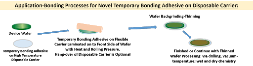
Wafer Processing Adhesives and Solutions
Thin semiconductor chips of 180µm thickness and below, even under 100 microns, are now quite common. The wafer processing required to achieve this level of thickness is correspondingly common. In the course of this processing, device wafers with finished integrated circuits must go through vigorous wafer backgrinding, polishing and stress relief with chemical and plasma processes.
With the advance of 2.5D and 3D device level packaging, the backside of the wafer must go through wafer processing that includes drilling, vacuum deposition and plating, lithography and various solvent and water cleaning processes. While the backgrinding and thinning process is normally considered separate from wafer processing, the ability to combine wafer backgrinding-thinning and backside active buildup will improve wafer throughput.

Backgrinding to thin out the device wafer and 2.5D-3D wafer processing on the thinned backside have many different processing steps. The temporary bonding adhesive on carrier supporting the processing must also have different adhesive characteristics such as bonding strength, and resistance to water, solvent, vacuum and temperature exposure. The temporary bonding adhesive must also be easy to de-bond on command, ideally without residuals for cleanup.
Multiplying Wafer Processing Throughput: Wafer Processing Adhesive on Disposable Carrier
AIT has developed temporary bonding adhesive on disposable carrier. Traditional temporary bonding adhesives for wafer processing have always required a carrier to match carrier-device wafer CTE during the rigors of processing. By eliminating the traditional glass carrier or silicon wafer carrier, wafer per hour throughput is greatly increased.
To successfully enable wafer processing with disposable carrier the key is the innovative, molecularly engineered temporary bonding adhesive: highly conforming, stretchable, and flexible temporary bonding adhesive yet with high shear bonding strength and high-temperature stability.
This novel solution cuts down the time, cost, and resources required for wafer processing by removing carrier bonding, carrier debonding, and carrier cleaning steps traditionally required.
These novel temporary bonding adhesives can also be used with traditional wafer processing glass or wafer carrier (hyperlink).
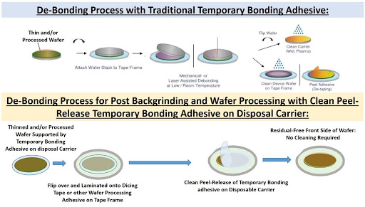
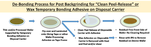
Infographic of the de-bonding process with traditional temporary bonding adhesive and glass carrier vs AIT patent-pending clean peel-release disposable carrier. The GD-PRCL-350 temporary bonding adhesive is engineered to have strong shear bond strength but sill peels cleanly from the device wafer. The adhesive remains attached to the disposable carrier throughout the process. The temporary bonding adhesive is molecularly designed to have the ability to conform and stretch to avoid interfacial stress and prevent finished wafer warpage.
With this clean peel-release adhesive, after finishing backgrinding and wafer processing, the carrier can be mechanically separated from the temporary bonding adhesive. The temporary bonding adhesive can simply be peel-release clean from the device wafer.
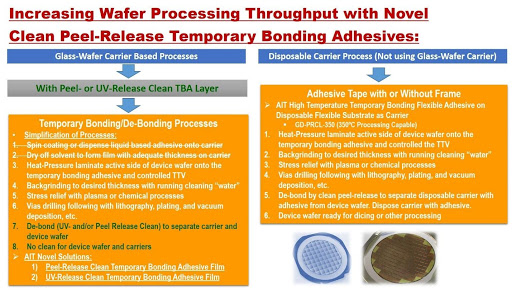
Temporary Bonding Adhesive Solutions with Clean Release De-Bonding:
Backgrinding and 3D Wafer Processing
AI Technology, Inc. created two novel temporary bonding adhesive solutions to simplify processing and increase the rate of wafer throughput:
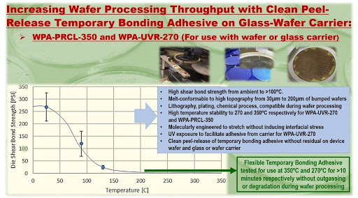
- Clean Peel-Release Stress-Free Adhesive Film: WPA-PRCL-350
- UV Clean Release Adhesive Film: WPA-UVR-270
Instead of using a more expensive and time-consuming focused laser to ablate the temporary bonding adhesive, WPA-UVR-270 enables the glass carrier to be released after UV exposure. The remaining temporary bonding adhesive film can be peeled cleanly from the device. Similar to the WPA-PRCL-350, there is no post-separation cleaning required. WPA-UVR-270 can be used for processing up to 270ºC while WPA-PRCL-350 can withstand wafer processing up to 350ºC.
These novel temporary bonding adhesives can also be used with traditional wafer processing glass or wafer carrier (hyperlink).
Wafer Processing for High Topography Bumped Wafers:
Conforming, Stress-Free Temporary Bonding Adhesive
AIT melt-conformal clean peel-release temporary bonding adhesive starts with the required thickness of 20µm for flat wafers. Temporary bonding adhesive thicknesses of 100µm, 200µm, and 400µm are made for stud bumps wafers and solder bumped wafers with adhesive total thickness variation less than 2µm.
- Melt-conforming-bonding process:
- temperature: 140-150ºC
- pressure: <14 psi or rolling lamination
Temporary bonding adhesive must melt and conform to absorb and encapsulate all of the bumps and features of the device wafer without stress. These criteria are critical for the success of backgrinding; if the adhesive does not meet these requirements the bumps will be reflected on the backside. AIT temporary bonding adhesive films WPA-PRCL-350 and GD-PRCL-350-WS, pre-deposited onto disposable carrier, have high melt-flow indices at 140-160ºC for ease of conforming to the highest of bumps, up to 200µm.
The following is an illustration of the two possible workflows for the 3D wafer processing using the AIT high conformable and high temperature capable clean release temporary bonding adhesives.
Film format availability for wafer processing temporary bonding adhesives eliminate dispensing, drying, and post leveling machining processes. Residue-free release from both the device wafer and carrier avoids cleaning processes and saves time, especially compared to focused laser ablation methods. The use of disposable carrier provides even greater efficiency.
The patent-pending solution with AIT melt-conformable temporary bonding adhesive wax on disposable carrier is molecular designed to have flexibility and conform without interfacial stress, including with disposal carriers, whether carrier has 7-9ppm/ºC to match CTE of SiC, Sapphire or GaAs wafer or otherwise. The wax adhesive film is available from 3µm and up.
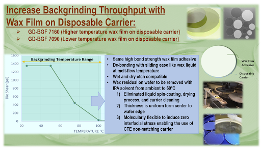
Backgrinding Wax Adhesive Solutions for SiC, Sapphire and GaAs Wafers
AIT wax film adhesives maintain more than 1000 psi shear bonding strength. The ability to hold the high shear bond strength up to 60ºC is important when backgrinding hard substrate wafers such as SiC (silicon carbide). High shear bond strength protects fragile wafer materials such as GaN and GaAs that can easily fracture with any stress concentration.
These novel wax film temporary bonding adhesives are also available pre-applied onto disposable carrier. The adhesive on disposable carrier is designed to provide the high shear bonding wax adhesive and disposable carrier to enable the multiplying of wafer throughput per hour. These proven wax film temporary bonding adhesives are now combined with disposable carrier with a finished total thickness variation of less than 2 µm.
Multiplying Wafer Backgrinding Throughput: Backgrinding Temporary Bonding Adhesive on Disposable Carrier
Traditional film-forming liquid waxes are preferred for their strong bonding to withstand vigorous shear force during backgrinding of hard wafer substrates such as SiC and Sapphire. It is also preferred to protect fragile wafers like GaAs from fracturing.
GD-BGF 7090 is a wax film pre-applied onto flexible disposal carriers (AIT patent-pending) that produces dramatic simplification of processing and thus results in much higher wafer backgrinding throughput.
GD-PRCL-200 is a novel melt-bonding temporary bonding adhesive that has outstanding shear bonding for backgrinding and peel-release-clean with no residual post backgrinding.
Wax film and melt-bonding flexible adhesive pre-applied onto disposable carrier can be melt-laminated onto the device or substrate wafer to be thinned.
Ease in de-bonding and cleaning are the keys for improving backgrinding throughput. The use of “clean peel-release” can provide multiplying factor to the backgrinding throughput of the difficult wafer such as SiC, Sapphire and GaAs.
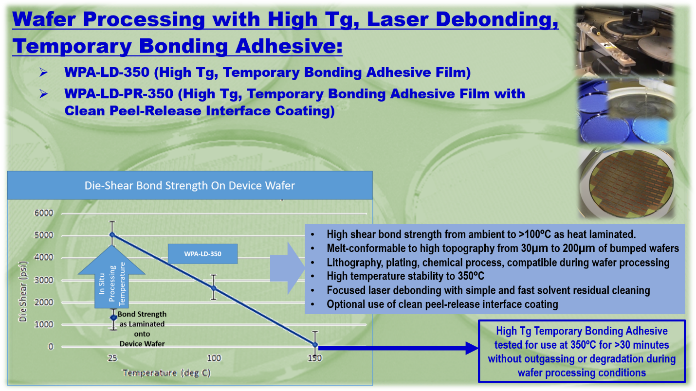
As melt-laminated onto the active side of the device, WPA-LD-350 create a high shear bonding between device wafer and glass carrier for vigorous backgrinding and polishing operations. The shear strength increases further with heating cycles in wafer processing while maintains thermoplastic compliance. This novel temporary bonding adhesive can be easily ablated with focused laser method for separation between the device wafer and the glass carrier. The residual layer can be removed within minutes with designed solvent mixture.
Laser De-Bonding, High Tg, Temporary Bonding Adhesive Solutions:
Focused laser debonding for separating device wafer from the glass carrier is the existing predominant method in the use of temporary bonding adhesive that has high Tg and modulus. AI Technology, Inc. has engineered the polymer structure to include high Tg at 240ºC, high thermal stability for beyond 350ºC wafer processing, and yet relatively low melt-lamination temperature at below 150ºC for adhesion and conformation with the bumped features on the wafer.
Molding Release Adhesive Tapes for Wafer and Panel Level Processing (FOWLP and FOPLP) and Heterogeneous Integration Molding:
Patented novel adhesive technology solutions for “clean release” no-clean molding release for panels up to 650mm. Flexibility in production use with pressure-sensitive adhesive integrated high temperature disposal carrier or double-sided adhesives for use with glass-wafer carrier.
AIT’s proven clean release technology allows for no-clean, high temperature processing and molding up to 265°C. The release adhesive layer is available from 20 to 200 µm in thickness for bumps and features of different heights and widths, up to 650mm. The release adhesive layer can also be ordered as heat releasing, UV releasing, or peel releasing to meet all processing requirements.
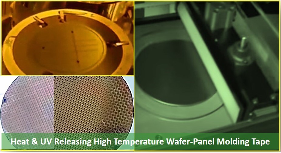
Patented novel “clean release”, “no-clean” pressure sensitive adhesive film-tapes for fan-out wafer and panel level 3D heterogeneous integration molding release applications. AIT innovated solutions include heat and/or UV release types with integrated disposable flexible carrier or double-side adhesive type for use with glass or wafer carrier. All of these AIT molding support adhesive tapes are applicable for processing and molding up to 265°C without residual upon release removal.