Temporary Bonding Adhesive Solutions with Clean Release De-Bonding: Backgrinding and 3D Wafer Processing
Current state-of-the-art wafer processing is summarized with the following process flow:
Spin coat or dispense liquid-based temporary adhesive onto carrier
Dry off the solvent to solid form or film
- Pre-machining may be needed to ensure suitable flatness
Heat-Pressure laminate active side of device wafer to the carrier
- Total thickness variation (TTV) controlled by parallel and flatness of the vacuum chuck and top press plate
Backgrind to the desired thickness with running cleaning water and surfactant
- Temporary bonding adhesive must not be affected by the water-surfactant
Stress relief of thinned device by plasma or chemical processes
- Temporary bonding adhesive be resistant to these processes
For 2.5D and 3D formation:
- Drill vias
- Processes of lithography, plating, vacuum deposition, etc.
- Temperatures may reach 350ºC and may involve vacuum or inert gas environments
- Temporary adhesive must be stable at these high temperatures and in these difficult environments
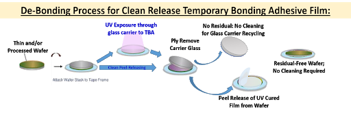
Separate device wafer from the carrier with focused laser, heat-sliding, or solvent soak
Clean device wafer and the carrier
- Lengthy cleaning with aggressive solvent
- Thus, wafer processing throughput is generally less than 20 per hour
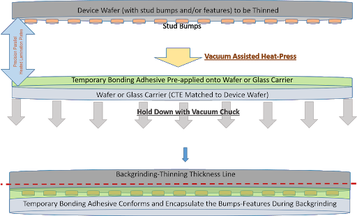
The above infographic represents the configuration of wafer processing with temporary bonding adhesive. Either wafer or glass carrier is used to support the backgrinding and wafer processing to minimize any warpage induced during high-temperature processing.
This process may be improved or simplified with innovation in the temporary bonding adhesive:
- Replace spin-coating or liquid deposition temporary bonding adhesive with a preformed temporary bonding adhesive film with tight total thickness variation.
- Temporary adhesive with the prerequisite strong bond strength but requiring no cleaning after debonding will dramatically increase the wafer per hour throughput
AI Technology, Inc. created two novel temporary bonding adhesive solutions to simplify the processing and increase rate of wafer throughput:
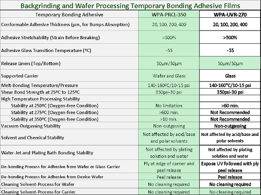
- Clean Peel-Release Stress-Free Temporary Bonding Adhesive Film: WPA-PRCL-350
- UV Clean Release Temporary Bonding Adhesive Film: WAP-UVR-270
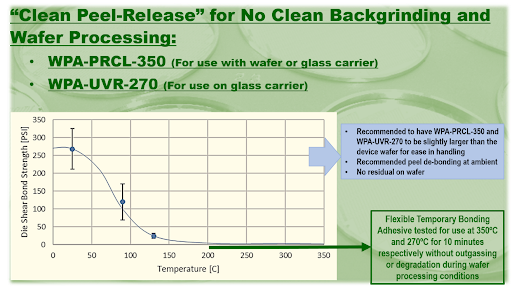
With this clean peel-release adhesive, after finishing backgrinding and wafer processing, the carrier can be mechanically separated from the temporary bonding adhesive. The temporary bonding adhesive can simply be peeled cleanly from the device wafer.
AIT novel temporary bonding adhesive can be used for direct heat-lamination onto either the device wafer or the supporting carrier. The de-bonding processes have been engineered to eliminate the need for cleaning post-separation.
Temporary bonding adhesives in film format simplify the adhesive application process. The adhesives’ clean release by peeling or UV eliminates the need for cleaning, multiplying wafer throughput.
Instead of using a more expensive and time-consuming focused laser to ablate the temporary bonding adhesive, WPA-UVR-270 enables the glass carrier to be released after UV exposure. The remaining temporary bonding adhesive film can be peeled cleanly from the device. Similar to the WPA-PRCL-350, there is no post-separation cleaning required. WPA-UVR-270 can be used for processing up to 270ºC while WPA-PRCL-350 can withstand wafer processing up to 350ºC.