A New Class of 3-D Wafer Buildup Prepregs
- New class build-up film adhesive technology with low dielectric constant and loss for high-speed circuit performance
- Proven molecularly engineered CTE to match copper for build-up flexibility
- Proven molecularly engineered stress relief High Tg modified cyanate ester technology
- Much lower moisture absorption and retention for reliability and circuit performance
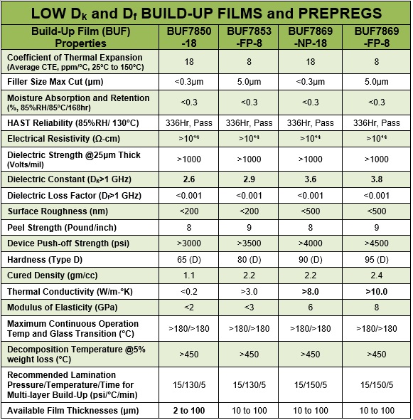
Low Dielectric Constant (Dk) and Loss (Df) while Maintaining Low CTE with Molecular Engineering:
In meeting the challenge of achieving higher electrical signal transmission at 5 to 6G frequencies, there is a difficult compromise between achieving controlled low CTE with quartz filling and still lowering the dielectric constant and loss from typical high Tg polymers. With proven polymer molecular engineering that AIT had achieved for other applications, a series of low Dk, low Df and low CTE are now developed for build-up film prepreg applications.
Features and Distinctions
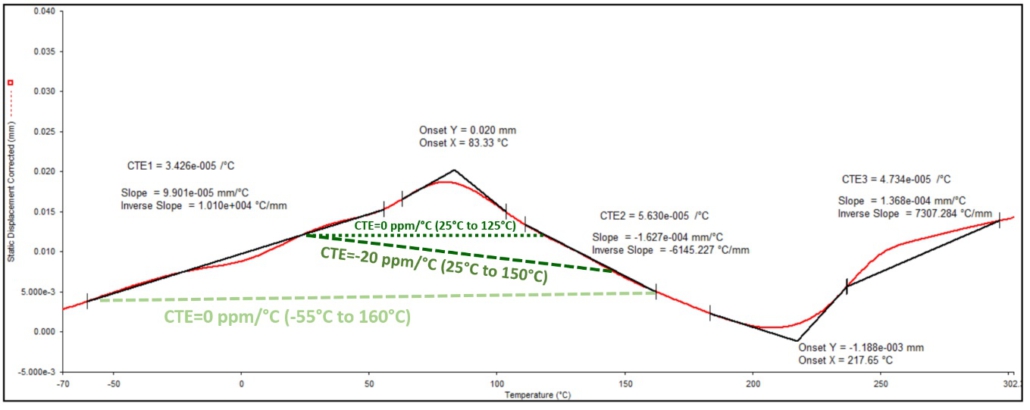
- Engineered CTE to less than 20 ppm/°C from 25°C to 150°C. Curing and laminating with copper and board substrate create no warpage or shear stress along the XY-plane and minimal Z-axis stress on copper stud and solder bumps.
- Modified cyanate ester to achieve less than 2.7 Dk for the low thermal dissipation applications while keeping it below 3.2 for those applications requiring thermal dissipation
- Industry first 3 μm build-up film thickness for even higher integration possibilities
- Molecularly engineered to absorb stresses inherently to prevent stress concentrations induced cracking and delamination
- Ultra-low moisture absorption for superior moisture resistance
- Low melt-bonding lamination temperature-pressure and shorter dwell time for high productivity
- High temperature stability to withstand soldering at 300°C
- Max Op Temp: >175°C
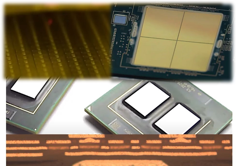
- Designed for fan-out wafer level processing (FOWLP) and fan-out panel-level processing (FOPLP) 3D devices