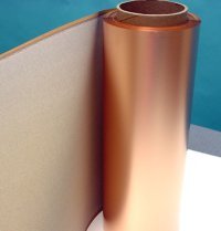
AIT COUPLER organic copper-clad laminate flexible circuit substrate and flexible circuit pre-preg material panels can be used to build one of the thinnest components and circuit boards with 40-50 micron dielectric over a 1/4 oz (9 micron) copper conductor.
COUPLER与AI Technology专有的柔性基材已被证明适用于:
- Through-hole plating for two sided interconnections
- Hydrophobic with ultra low moisture absorption
- Low dielectric constant
- No volume limitation
Solderable Flexible Circuit Materials For Fine-Pitch And Super-Fine Pitch Flexible Circuit Applications
AI Technology has developed a solderable, organic copper-clad laminate flexible circuit substrate materials that can be used at temperatures as high as 300°C. The standard flexible circuit material uses 1 oz copper on this non-polyimide proprietary molecularly flexible material for a total 3-mil thickness as flexible circuit substrate. These flexible circuit materials are available with 1/4 or 3/8-oz copper for super fine-pitch flexible circuit applications of less than 1-mil line/spacing and via.
COUPLER™ Flexible Circuit Material Characteristics:
- Proprietary organic copper-clad laminate material with low dielectric constant, 3.0 @ 1 KHz with less than 0.01 dielectric loss and high insulation strength (>1000VDC/3-mil thickness).
- Non-silicone and non-contaminating molecularly flexible dielectric layer.
- Withstands chemical etching and wet chemical treatments for all PWB/PCB processes.
- Maintains outstanding flexibility even at temperatures of as low as 40°C.
- Eliminates traditional polyimide flexible circuit material “measling” and other moisture induced degradation and reliability problems as usually associated with polyimide based circuit boards.
- Outstanding moisture resistance, less than 0.3%, while maintaining high electrical and mechanical performance.
- UL-94-V0 fire-retardant rating.
- Same circuit density and design rules as traditional FR-4 and BT board.
- Lower temperature multi-layer flexible circuit processing from as low as 125°C.
- Solderable flexible circuit applications at 50% of the traditional polyimide flexible circuit material substrate cost.
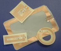
Applications:
- Organic copper-clad laminate substrate flexible circuit materials to replace polyimide and PTFE.
- Flex tape for area-array flexible circuit and interposer substrate.
- Flip-chip on flex with superfine pitches.
- Directly solderable flat and flexible jumpers.
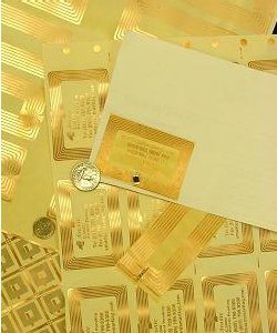
- 扁平而灵活的布线,可在班级中使用。
- 可焊接的薄膜开关和电路。
- 辊对辊或面板加工。
- 可提供不同长度和宽度的卷筒。
AI Technology COUPLER™有机覆铜板柔性电路基板和柔性电路预浸料板的处理方法和基础结构与标准PWB和柔性电路常用的方法和基础结构完全相同。
1.板材和卷材处理
- COOL-CLAD™和COUPLER™有机覆铜板柔性电路基板可在环境条件下至少保存12个月。
- COUPLER™柔性电路预浸材料在环境条件下至少可储存6个月。
2.面板准备工作
- 工具/注册
- 擦洗
- 化学清洗
- 基本金属保护
3.3. 成像
- 干膜应用
- 湿膜应用
- 筛选后的图像应用
4.湿式化学处理
- 蚀刻
- 剥皮
- 蚀刻后/剥离清洗
5.焊锡面罩的应用
- 筛网、喷涂或科汀涂料
- 热焊接掩模
- 紫外光固化焊剂面膜
6.第二步钻孔或打孔
- 冲床
- 钻机
- 7.完成作业
- HASL
- OSP
- 锡
- Ni/Au
8.精加工制造
- 路线
- 得分
- 冲床
| 特征 | 单位 | 调理 | 典型值 | 规格 | |
|---|---|---|---|---|---|
| 体积电阻率 | M&-cm | C-96/35/90 | 5X10⁸~5X10⁹ | 106 | |
| 表面电阻率 | M& | C-96/35/90 | 5X10⁶~5X10⁷ | 10t | |
| 许可率1MHz | – | C-24/23/50 | 3.8-4.2 | 5.4 | |
| 损耗切线 1 MHz | – | C-24/23/50 | 0/013-0.020 | 0.035 | |
| 弧线阻力 | 秘书部 | D-48/50 + D-0.5/23 | 100 | 60 | |
| 绝缘体分解 | KV | D-48/50 | 45 | 40 | |
| 吸湿性 | % | D-24/23 | 0.01-0.20 | 0.35 | |
| 可燃性 | – | C-24/23/50+E-24/125 | 94V0 | 94V0 | |
| 去皮强度1盎司 | Lb/in | 288°C浮焊 | 8 | 8 | |
| 热应力 | 秘书部 | 288°C 焊剂浸渍 | 600 | 300 | |
| 压力锅(2 atm/120°C) | HR | HR | 秘书部 | 288°C 焊剂浸渍 | 300 |
| 1小时 | 秘书部 | 288°C 焊剂浸渍 | 300 | 不适用 | |
| 2小时 | 秘书部 | 288°C 焊剂浸渍 | 300 | 不适用 | |
| 抗弯强度 | LW | 磅礴 | A | 6000 | 60000 (不适用,用于柔性电路) |
| CW | 磅礴 | A | 5000 | 60000 (不适用,用于柔性电路) | |
| X-Y轴的尺寸稳定性 | % | E-0.5/170 | 0.01-0.020 | 0.050 | |
| 热膨胀系数 | Tg以下的Z轴 | 英寸/英寸/℃ | TMA | 60 PPM | 不适用 |
| Z轴高于Tg | Z轴高于Tg | 英寸/英寸/℃ | TMA | 180 | 不适用 |
| 玻璃过渡温度 | °C | DSC | -40 +/- 5 | 不适用 |
欲了解更多信息和推荐帮助,请联系AI Technology销售和工程部。
![]()
AIT technical sales and service department can also be reached at: 1-609-799-9388 and Fax: 609-799-9308