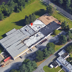
AI Technology, Inc. Headquarters – 70 Washington Rd. Princeton Junction, NJ 08550
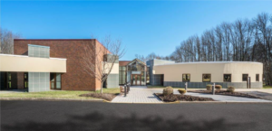
AI Technology, Inc. Second NJ Facility – 18 Roszel Rd. Princeton, NJ 08540
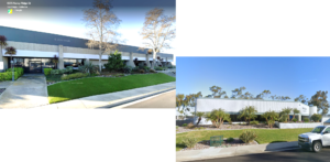
Ormet Circuits – 6555 Nancy Ridge Rd., Suite 220 San Diego, CA 92121
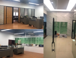
AI Technology, Inc. Asian Operations
公司的使命:提供满足客户需求的产品,是美亚科材不变的宗旨!
AI Technology在使用先进材料提供电子封装领域的前沿解决方案方面有着令人骄傲的历史。 随着20世纪80年代率先将分子柔性环氧树脂胶粘剂用于芯片和基底粘接,30多年来的卓越可靠性已经证明了使用顺应性和非硅胶粘剂的好处。使用柔性环氧树脂胶粘剂薄膜和浆料粘合剂处理大面积的粘接以提高半导体器件的长期可靠性,现在已成为管理界面应力的公认 "黄金法则"。
AI Technology, Inc. (AIT), founded in 1981 and commencing manufacturing operations in 1985, has grown to become a leading provider of advanced electronic packaging adhesives and material solutions. AIT is headquartered on a 16-acre manufacturing and R&D campus in Princeton Junction, New Jersey. In 2022, AIT expanded its production and research capabilities with the addition of a second, company-owned 18-acre campus in Princeton, NJ. AIT manufactures products to ISO 9001:2015 standards and has maintained this accreditation since 1999.
Over more than 40 years of organic growth, AIT has developed one of the most comprehensive lines of film and paste adhesives, enabling customers to build products with exceptional reliability and cost efficiency. Since pioneering low-modulus, low-stress adhesive paste and film technologies, AIT has continued to expand its offerings to include semiconductor and electronic packaging adhesives, underfill materials, encapsulants, and coating solutions.
AIT has a proud history of delivering leading-edge solutions in electronic packaging through the use of advanced materials. Pioneering the use of molecularly flexible epoxy adhesives for die and substrate attaches in the 1980s, AIT demonstrated the proven benefits of compliant, non-silicone adhesives, with over 25 years of exceptional reliability. Today, the use of flexible epoxy and cyanate ester adhesive films and pastes for large bonding areas is widely regarded as the “golden rule” for managing interfacial stresses and enhancing long-term semiconductor device reliability.
Key Milestones in AIT’s Development and Growth
- 1981: Incorporated by Dr. Kevin Chung.
- 1985: Began manufacturing operations, producing EMI/RFI shielding caulks, gaskets, adhesives, and conductive coatings for extreme environments.
- 1985–Present: Pioneered Non-Silicone, Flexible, Stress-Free Epoxy and Film Technology for microelectronic packaging.
- 1985–Present: Developed one of the most comprehensive lines of microelectronic film and paste adhesives, thermal interface materials, coatings, and materials, including many products certified to Mil-Std and NASA outgassing standards.
- 1990–Present: Pioneered the first Self-Supporting Die-Attach Film Adhesive for stacked-chip applications.
- 1998: Relocated to a company-owned 16-acre site with a 52,000 sq. ft. manufacturing and R&D facility in Princeton Junction, NJ.
- 2000–Present: Cool-Grease CGR7016/CGR7018 became the standard for RIE and high-temperature wafer processing.
- 2011–Present: Patented SOLAR-THRU™ PVDF-based front-sheet films and thermally conductive back-sheet technologies for advanced solar energy applications.
- 2015–Present: Introduced wafer processing temporary adhesives (waxes and specialty films) for applications ranging from ambient to 350°C.
- 2016–Present: Launched FLUOROSEAL® and CIRCUITSEAL®, proven IPC-certified 830C conformal coatings for corrosion prevention.
- 2020–Present: Developed nano-conductive coatings for precision, component-level EMI protection.
- 2021: Expanded operations with a 46,000 sq. ft. clean-room facility and R&D center at 20 Roszel Road, Princeton, NJ.
- 2022: Established the AITCOATINGS division to deliver patent-pending PVDF-based corrosion protection coatings for industrial, commercial, and consumer applications.
- 2023: Introduced advanced Wafer Level Temporary Bonding and Packaging Solutions, including UV ablation, UV-activated release, peel release, heat release TBDB, BUF film adhesives, fine-pitch underfills, and wafer protection film adhesives.
- 2024: Acquired Ormet Circuits Inc., expanding AIT’s portfolio with unique TLPS technologies for high-density interconnect (HDI) and high-temperature advanced electronic packaging applications.
AIT Today
AIT serves worldwide customers across the semiconductor, die-component-substrate level packaging, circuit board conformal and corrosion protection coating, and device-level EMI/RFI shielding markets. Key strengths include:
- ISO Certified Facilities and manufacturing processes.
- Over 40 U.S. patents in microelectronics materials.
- A team of 5+ Ph.D.-level materials scientists and chemists dedicated to product development.
Since the 1990s, AIT has maintained a strong global presence, with local staff providing dedicated product support to customers in Hong Kong, Taiwan, and Shenzhen, along with long-standing partnerships across Europe and Asia.
We actively welcome inquiries to collaborate with local partners to deliver reliable solutions, including electronic adhesives, thermal interface materials, EMI shielding materials, flex circuit substrates, semiconductors, and wafer processing tapes and materials. Backed by our experienced team of engineers, scientists, and product support professionals, AIT is committed to providing innovative, high-quality solutions tailored to enhance customer productivity and performance.
AIT technical sales and product support department can also be reached at: 1-609-799-9388 and Fax: 609-799-9308